AMD recently bought Taalas, a quiet startup with a radical idea: stop running AI models on general-purpose processors, and start baking them directly into the silicon gates.
For the last few years, the tech world has operated under a single assumption. To run AI, you need GPUs. You buy thousands of Nvidia or AMD chips, load your model weights into high-bandwidth memory (HBM), and run software that tells the chip how to compute the math. It works, but it is incredibly wasteful.
GPUs are the Swiss Army knives of computing. They are designed to be programmable because nobody knew which AI architectures would win five years ago. But programmability carries a heavy tax. You pay for it in power, silicon space, and billions of dollars in memory costs.
As AI models mature and stabilize, we are entering a new phase. We do not need programmable chips to run a model that will not change for the next two years. We need chips that do one thing fast and cheap. That is where Taalas comes in, and why AMD spent real money to acquire them.
The Memory Wall and the GPU Tax
To understand why hardwiring models matters, you have to look at how a GPU actually runs an LLM.
When you type a prompt into an AI, the GPU has to fetch the model's weights from its memory, bring them to the compute units, perform the math, and send the result back. This happens for every single token generated.
The physical distance between the compute units and the memory is the biggest bottleneck in AI today. Moving data across a chip takes vastly more energy than the actual math. This is called the memory wall. It is why modern GPUs require massive stacks of HBM, which are expensive to make and run hot.
If you look at a modern GPU die, a huge portion of the silicon is not even doing math. It is dedicated to memory controllers, instruction decoders, cache hierarchies, and scheduling logic. All of that exists just to support programmability.
If you are running a fixed model like Llama-3 in a customer service bot 24/7, you do not need programmability. You are paying for a massive infrastructure on the chip that you never use.
How Etching Models Works
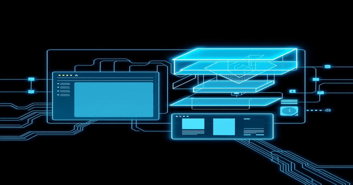
Taalas built a compiler that skips the software layer entirely. Instead of writing code that runs on a chip, their software takes a deep learning model and translates its architecture directly into a hardware design.
The weights and the connections of the neural network become physical wires and gates on the silicon.
In a standard chip, you load weights from memory into registers to multiply them. In an etched chip, the weight is represented by the physical layout of the transistors. The data flows through the chip like water through a custom-built pipe system.
This approach changes the math of chip design:
- No HBM Required: Because the weights are baked into the logic gates, you do not need gigabytes of ultra-fast external memory. The memory bottleneck disappears.
- Massive Power Savings: Without data constantly traveling back and forth between memory and compute, power consumption drops by orders of magnitude.
- Smaller Die Size: You can strip away the instruction decoders, schedulers, and cache. The resulting chip is a fraction of the size of a GPU, meaning you can print far more of them on a single wafer.
Instead of a 700-watt GPU that costs $30,000, you get a small, cheap ASIC (Application-Specific Integrated Circuit) that runs at 10 watts and costs a few dollars to manufacture at scale.
The Obsolescence Risk
The obvious objection to hardwired AI is flexibility. If you etch Llama-3 into a chip, and Llama-4 comes out next month, your chip is suddenly obsolete. You cannot run a firmware update to change the physical wiring of the silicon.
This is a real risk, but it matters less than it used to.
We are reaching a point where certain model sizes and architectures are becoming "good enough" for specific tasks. A bank using a model for fraud detection does not need the latest creative writing capabilities of a frontier model. They need their specific, audited model to run millions of times a day as cheaply as possible.
There are also ways to build semi-programmable ASICs. You can etch the core weight matrix into the silicon but leave small, programmable blocks at the edges to handle minor tuning or weight updates. This gives you 90% of the efficiency of a fully hardwired chip while keeping some ability to adapt.
Even if a chip is completely static, the economics still work. If an etched chip is 50 times cheaper to run than a GPU, it pays for itself in a matter of months. If a better model comes out next year, you throw the old chip away and print a new one. The total cost is still lower than renting GPU instances in the cloud for the same duration.
AMD's Post-GPU Strategy
AMD is currently fighting a hard battle against Nvidia in the data center GPU market. The MI300 series is selling well, but Nvidia still commands the software ecosystem with CUDA.
Buying Taalas gives AMD a way to bypass the CUDA moat entirely for inference workloads.
If AMD can offer enterprise customers a pipeline where they train their models on AMD GPUs, and then compile those models directly into custom silicon, they change the dynamics of the market. Customers no longer have to worry about GPU availability or cloud rental costs. They can deploy their proprietary models on-premise, in edge devices, or in cars using custom chips designed by AMD's new tooling.
This also fits perfectly with AMD's chiplet technology. AMD is a leader in mixing and matching different pieces of silicon on a single package. They could easily package a small, etched Taalas AI block alongside a standard Ryzen CPU or EPYC server chip.
The Shift to the Edge
The real battleground for etched silicon is not the cloud data center. It is the edge.
Running local models on phones, laptops, smart home devices, and cars is currently limited by battery life and thermal limits. You cannot put a GPU in a security camera or a smartwatch. But you can put a tiny, 1-watt etched chip that runs a specific voice recognition or object detection model.
By baking models into silicon, we can bring intelligence to devices that have no internet connection and very little power. It makes AI local, private, and instantaneous.
AMD's acquisition of Taalas suggests they see this transition coming. The era of running every single AI query through a massive cloud data center is unsustainable. The grid cannot support the power requirements, and the latency is too high for real-time applications.
Etching models into silicon is the logical end state for mature AI workloads. We did the same thing with video decoding, cryptography, and graphics routing. We started with software on general-purpose chips, and we ended with dedicated hardware blocks. AI is simply following the same path.